公司简介
Provides thin-film coating employing multiple PVD techniques. Types of coatings include infrared (SWIR to LWIR), resistive, EMI, RFI, static, dissipative, transparent conductive, and patterned. Chambers to 14 ft length, pattern generation types, photolithographic (etch back and lift off, dry etch, shadow mask).
技术能力
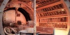
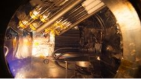
Electron Beam (With Flip Tool) | Buellton Advanced Materials PVD Coatings Electron BeamOur chambers have multi-hearth sources allowing for multiple materials to be deposited without having to break vacuum to atmosphere and to be applied in one continuous process. Specialized chambers allow 360 degree coating coverage, also equipment setup with specialized tooling to allow for coating of two sided substrates without breaking vacuum. BAM's larger coaters are setup with 5 and 6 electron beam guns respectively for large area highly uniform coating coverage |
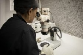
QC Product Inspection | Thermal EvaporationUtilizing a resistance heater to melt the material and raise its vapor pressure to a useful range. Useful for materials that may disassociate using electron beam deposition - such as ZnS, YF3. SputterOur sputter tools are configured to deposit up to three material types per coating run without breaking vacuum, providing the best quality of film stack. BAM has a dedicated Indium Tin-Oxide tool that can deposit highly optically transparent ITO onto plastic as low as 15 ohm's/square and at near ambient temperatures, allowing us to apply this type of film without distorting or damaging the plastic. |
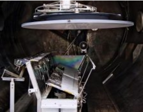
Parabola Metallization | General Coating CapabilitiesFlex/KaptonSubstrates: Kapton, multilayer flex |
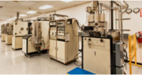
PVD Coating Line | Ceramic MetallizationTypical ceramics: AlO, AlN, BeO |
Specialized Tooling (360 Degree Coverage) | Eutectic and Solder MetallizationAu/Sn, In/Cu, Au/Ge, In Rigid: Composite/PlasticsTypical substrates: Astroquartz, PEEK, ULTEM |
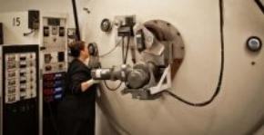
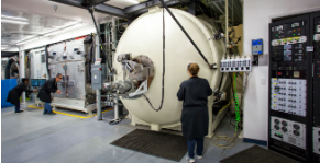
Large Area Coatings (High Volume/Large Parts) | TCO: Transparent Conductive Oxides Standard material: ITO (Indium Tin-Oxide) Compound Curves and 360° Wrap Around Coated PartsTypical substrates: No typical substrates (non-symmetrical shapes) |
Large Area Coatings | Optical CoatingsWavelengths: SWIR - LWIR typical 1 – 14µm (2016 / 2017 Capa |


