公司简介
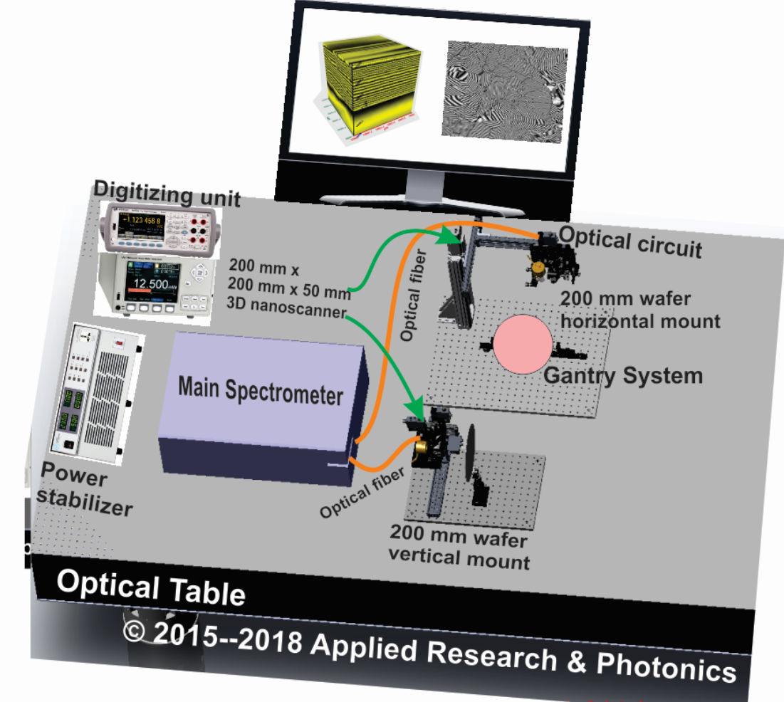
Applied Research & Photonics, Inc. (ARP) provides terahertz nano-scanning material characterization testing services and technology to semiconductor and nano-material researchers and manufacturers. Their TeraSpectra Spectrometer is a sub-surface nano-scanner and 3D imager that provide non-contact, non-destructive testing capabilities at ambient temperatures.
产品列表
TeraSpectra: A terahertz spectrometer
ARP’s Terahertz Spectrometer, TeraSpectra is a turn key spectrometer system, that allows time domain measurements to be conducted over a time span of sub-Pico seconds to a few tens of Pico-seconds with an equivalent frequency range of 0.1 to ~30 THz.
This wide range allows characterizing a number of molecular events important in semiconductor and nano-material research and inspection.
| Parameter | TeraSpectra |
|
| Time resolution | ~33 Femto-seconds | |
| Time span | Up to 100 Pico-seconds | |
| Fourier Transform Frequency Range | 0.1 up to ~35 terahertz | |
| Technology | Next generation EO dendrimer terahertz emitter | |
| Source power | >5 milliwatts, average | |
| Sensitivity | ~100 FemtoMol |
Key Features
Turn-key System
3-Dimensional Imaging
Sub-Surface Inspection
Non-Contact
Non-Destructive
Layer-by-Layer Analysis
Material Characterization:
Lattice Image
Stacking Fault
Dislocations
Nanovoids
Delamination
Testing Services
Semiconductor & Nanomaterial Testing Services
Applied Reseach & Photonics, Inc. (ARP) provides terahertz nano-scanning material characterization and testing services that helps semiconductor and nanomaterial researchers and manufacturers, easily visualize and identify in 3-Dimensional images, surface, sub-layer defects and failures. ARP testing is non-contact, non-distructive and performed at ambient temperatures.
New Innovative Imaging Technololgy
ARP’s Terahertz Scanning Spectrometer (TeraSpectra) is a Terahertz Nano-Scanning Spectrometer/3D Imaging system that has two key technology innovations:
1) it breaks the spatial resolution limit of current generation optical inspection technologies, and
2) it uniquely identifies location and depth where defects exist.
Currently, there is no measurement technology that has the capability to provide an equivalent richness of information that ARP’s TeraSpectra system can deliver without damage or destruction of the test sample.
Current Inspection Technology have Limitations
Atomic Force Microscopes (AFM) are one of the go-to technologies for wafer inspection, but require surface contact which can damage nanometer scale circuits. X-Ray inspection technology imparts high energies which can damage substrate lattice structure. IR inspection technologies at wavelengths of 1.5 microns and UV inspection at 256 nanometers, which are the current state of the art, but are limited to surface inspection only. Electron Microscopes are very expensive, require sample destruction and tedious sample preparation.
Materials
Semiconductor Wafers
Nanomaterials
Soft materials
Nano-composites
Key Features
3-Dimensional Imaging
Sub-Surface Inspection
Non-Contact
Non-Destructive
Layer-by-Layer Analysis
Material Characterization:
Lattice Image
Stacking Fault
Dislocations
Nanovoids
Delamination
Fast Turnaround Testing
Once material samples are received test duration is typically between 1 and 3 days per sample. Test duration, as always, are subject to the test criteria and characterization requirements of our customers. ARP consultants provide a comprehensive test report and assist in interpretation of results.
Image Gallery
Quantum Dots with nanometer resolution
(a) 100 nm3 volume of AgI quantum dots on Si wafer (b) three different layers extracted from (a)
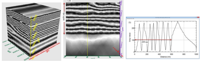
Chromin Salt nanoparticles – Sub-nanometer image resolution

(a) 100 nm2 area of chromim salt nanoparticles on glass slide. (b) Close up. (c) Graphical analysis of a small single grain showing <1 nm size.
Lattice stacking fault in grown semiconductors
(a) Lattice stacking fault. (b) Planar image showing lattice planes and boundary. (c) Graphical analysis of dimensions.
Carbon Nanotube Film

Carbon nanotube film on Si wafer: (a) unaligned (b) 60° aligned
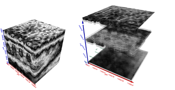
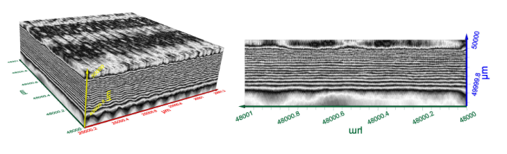
GaN on SI Wafer

(a) Three dimensional image of 1 cubic micron volume of a “GaN on Si” wafer. (b) One square micron surface image of the same (YZ plane). Distorted lattice patterns are visible indicating damages of the GaN layer.
Graphene
(a) 3D image of graphene exfoliate layers on Si wafer. (b) A single side (YZ surface) extracted from (a)
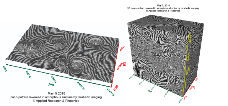
Amorphous Alumina